Nanolasers
Plasmonic devices exploit electromagnetic waves known as surface plasmons that propagate at the surface of a metal. Because these waves allow light to be concentrated in nanometer-scale volumes (or “hot spots”), they can lead to enhanced light–matter interactions (e.g. enhanced absorption, scattering, fluorescence, optical nonlinearities, etc.). Consequently, patterned metallic films have been studied for various photonic applications including photocatalysis, sensing, solid-state lighting, and solar cells.
However, because surface plasmons involve electron motion in the metal that dissipates energy, these waves also suffer from intrinsic losses that severely limit light–matter interactions and the performance of plasmonic devices. Therefore, simple routes to counteract losses by adding a gain material to rejuvenate the surface plasmons have been sought. Moreover, by adding sufficient optical gain to a plasmonic resonator, a "spaser" can be created. A spaser is the plasmonic analog of a laser (i.e. it provides a source of coherent surface plasmons instead of light). This can lead to an extremely versatile nanoscale source of surface plasmons, photons, and/or intense electromagnetic fields, depending on the design. Therefore, spasers can enable fundamental studies on the limits of nanoscale optics as well as applications in a broad range of areas, including hyper-spectral imaging, spectroscopy, and sensing.
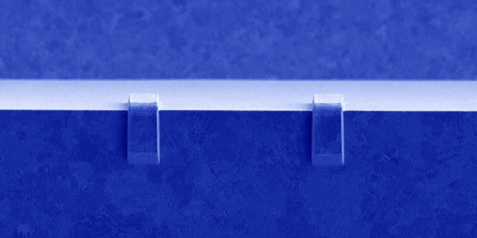
To explore all of the topics discussed above, researchers in OMEL have been exploiting our expertise in two key areas: (a) highly fluorescent semiconductor nanocrystals and (b) high-quality low-loss patterned metallic films.1,2 By combining these, we can pursue both interesting physics and potentially useful devices. We develop state-of-the-art designs and fabrication processes to create quantum-dot-decorated plasmonic devices.3 We then investigate their photophysical behavior. In addition to applications, these projects sometimes push into the realm of quantum mechanics where light and matter become strongly mixed.4 Thus, we are always on the lookout for unexpected phenomena.
1. Nagpal, Lindquist, Oh, & Norris. Ultrasmooth Patterned Metals for Plasmonics and Metamaterials. Science 325, 594 (2009). (external page Link)
2. McPeak, Jayanti, Kress, Meyer, Iotti, Rossinelli, & Norris. Plasmonic Films Can Easily Be Better: Rules and Recipes. ACS Photonics 2, 326 (2015). (external page Link)
3. Kress, Antolinez, Richner, Jayanti, Kim, Prins, Riedinger, Fischer, Meyer, McPeak, Poulikakos, & Norris. Wedge Waveguides and Resonators for Quantum Plasmonics. Nano Letters 15, 6267 (2015). (external page Link)
4. Winkler, Rabouw, Rossinelli, Jayanti, McPeak, Kim, le Feber, Prins, & Norris. Room-Temperature Strong Coupling of CdSe Nanoplatelets and Plasmonic Hole Arrays. Nano Letters 19, 108 (2019). (external page Link)